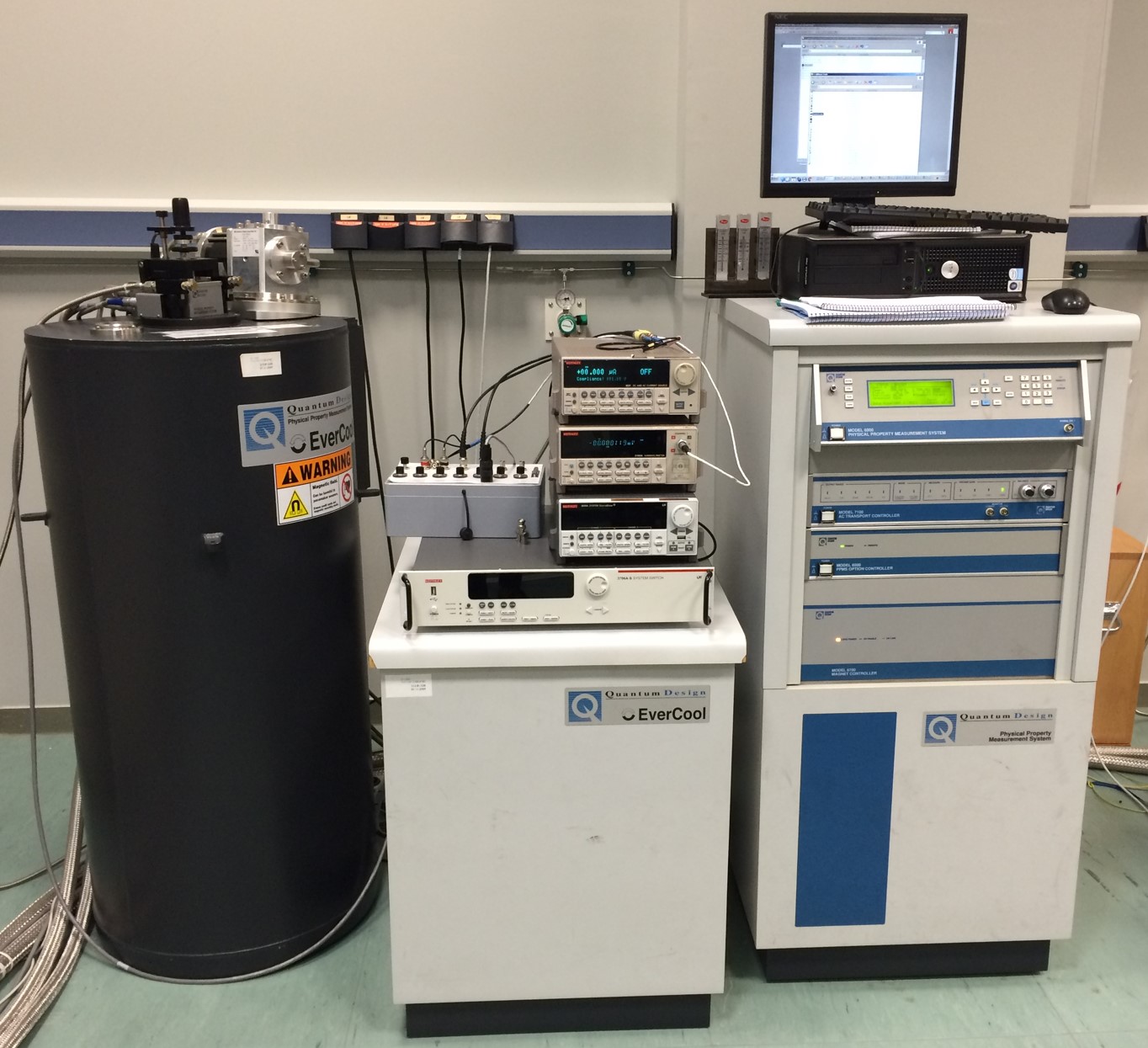
Electrical characterization
Electrical characterization
What we can offer:
-
Resistance versus temperature (2K - 400K).
-
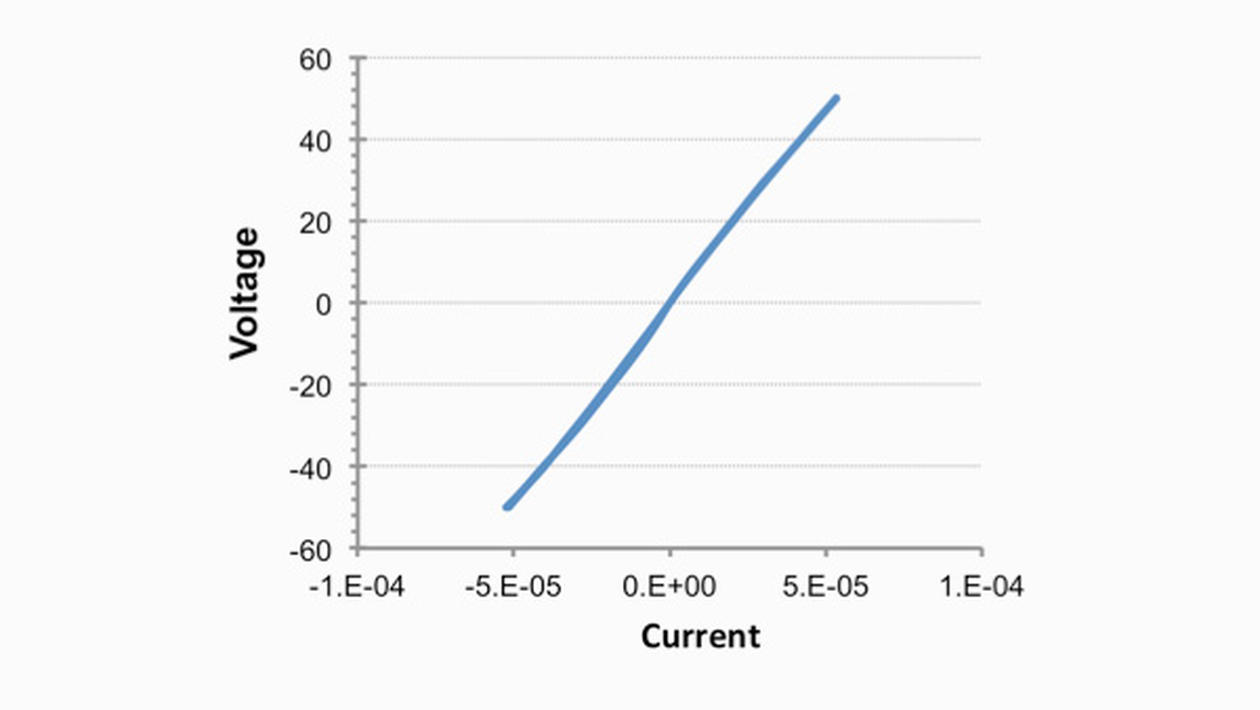
I(V) and V(I) curves at different temperatures (2K - 400K) applied filed up to 9T.
-
Magneto resistance measurements.
Possibility to:
-
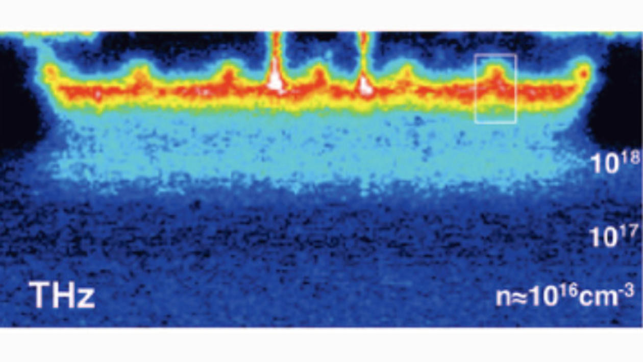
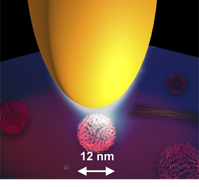
Mapping of local conductivity and identification of materials in semiconductor devices and/or nanowires.
-
Molecular disorder in organic semiconductors.
-
Detailed electrical properties characterization in newly synthesized or modified materials (thin films, particles...).
-
Sheet-resistance measurement of thin films and surfaces.
-
Nano/micro electronic-devices complete characterization.
Interesting for:
Semiconductor industry, biotech, materials-science industry, iron ad steel industry, metallurgy, machine-tool manufacturers, microelectronics and microsystems companies...
Cleanroom
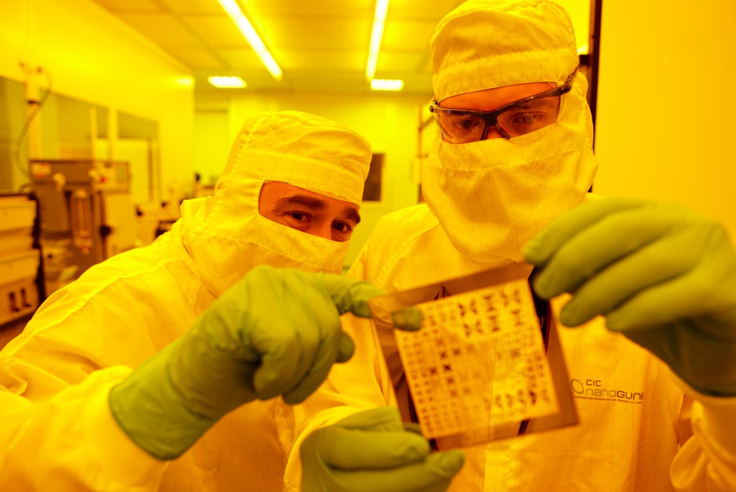
The nanoGUNE cleanroom, dedicated to fabricate and characterize the properties of materials on the nanoscale, ia a 300m2 laboratory where the air purity is under strict supervision.
Equipment
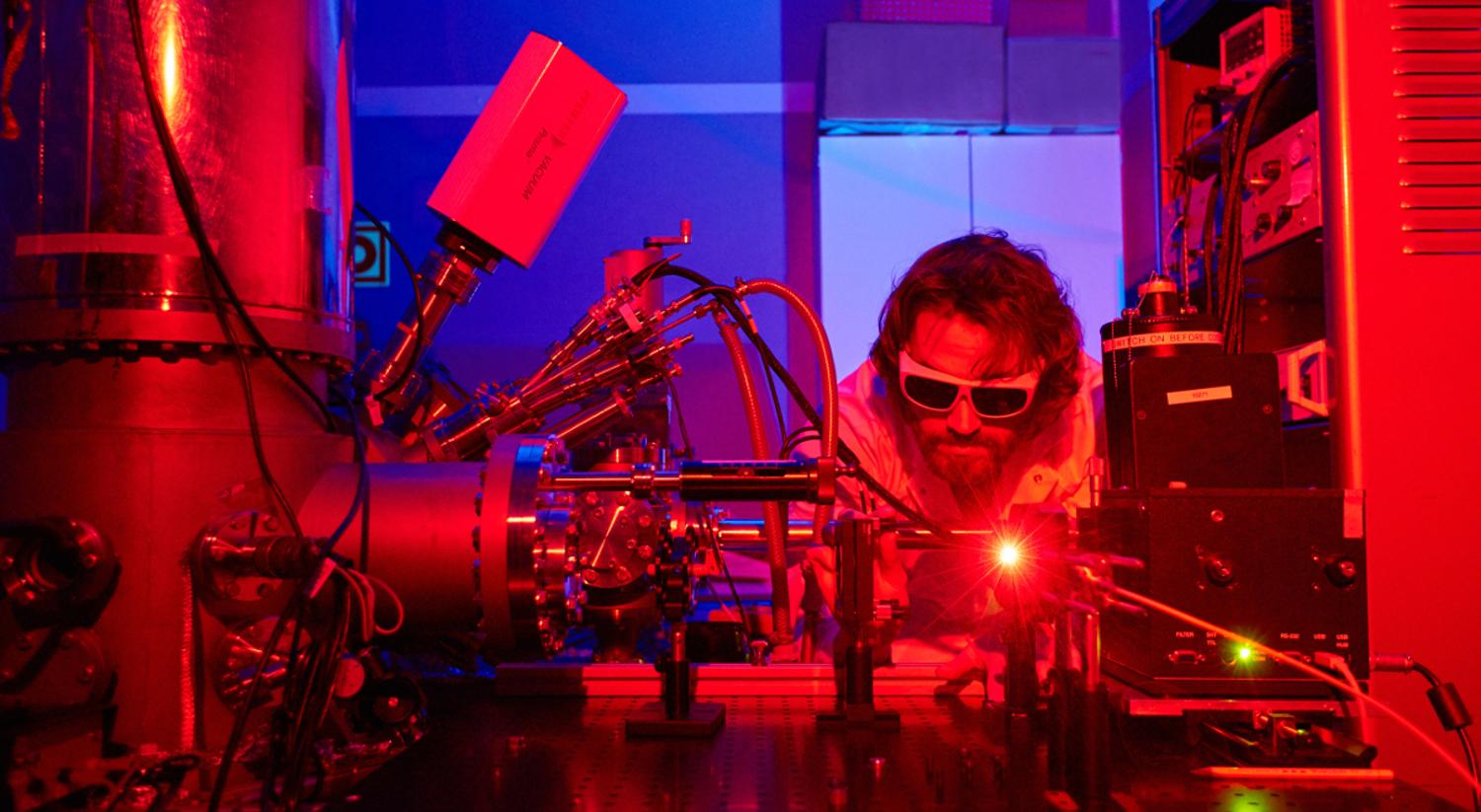
State-of-the-art equipment, including electron and scanning-tunneling microscopes, as well as other nanofabrication and characterization tools, are managed by specialists and used by researchers from a wide variety of fields.
Cleanroom
The nanoGUNE cleanroom, dedicated to fabricate and characterize the properties of materials on the nanoscale, ia a 300m2 laboratory where the air purity is under strict supervision.
Equipment
State-of-the-art equipment, including electron and scanning-tunneling microscopes, as well as other nanofabrication and characterization tools, are managed by specialists and used by researchers from a wide variety of fields.