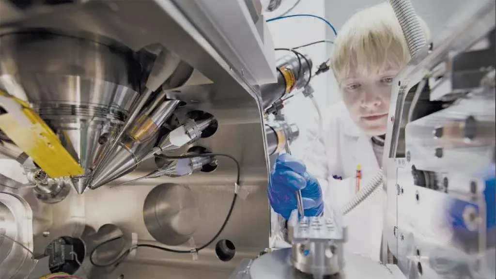
Electron Microscopy Platform
Usage
Electron Microscopy Platform
- Understanding the (miss)behavior of materials
- Atomic-resolution imaging, crystalline structure, stress analysis, grain size distribution, micro/nano tomography (3D images), surface morphology
- Silicon polished samples for calibration