Visualizing Energy Transport in Nanostructured Semiconductors
Speaker
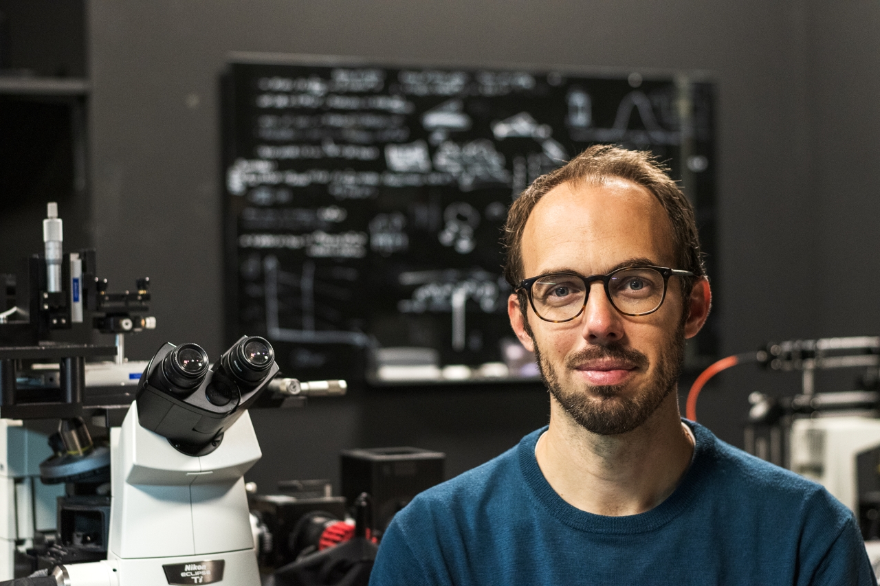
Ferry Prins
Affiliation
U Autónoma Madrid
When
Place
CIC nanoGUNE Seminar room, Tolosa Hiribidea 76, Donostia-San Sebastian
Host
Beatriz Martín-García
Nanostructured Semiconductors are a playing an increasingly dominant role for next-generation light-harvesting and light-emitting applications. In these materials, quantum confinement effects allow for enhanced control over their optoelectronic properties while reduced processing temperatures provide routes to more flexible integration. However, the reduced dimensionality and increased disorder can significantly impact the spatial dynamics of the energy carriers within the material.[1]
To study these effects, we employ Transient Photoluminescence Microscopy techniques which allow for a direct visualization of the excited state transport with few-nanometer and sub-nanosecond resolution. In this talk, I will highlight some of our recent efforts using this technique, with an emphasis on perovskite semiconductors of varying compositions and dimensionality. I will start the talk by giving an overview of some of the surprising effects that can be observed in these materials, particularly regarding the relationship between lattice softness and the exciton transport properties and the remarkably efficient interlayer transport.[2,3,4] In a second part of the talk, I will present results on mixed-halide 2D perovskites.[5] Halide mixing is one of the most powerful techniques to tune the optical bandgap of metal-halide perovskites across wide spectral ranges. However, halide mixing has commonly been observed to result in phase segregation, which reduces excited-state transport and limits device performance. In our work, we study the specific case of 2D metal-halide perovskites, in which phase segregation is absent. Importantly, our results show that even in the absence of phase segregation, halide mixing still impacts carrier transport due to the local intrinsic inhomogeneities in the energy landscape.
In the last part of the talk, I will present our most recent efforts using interferometric scattering techniques to study perovskite semiconductors. The exceedingly high signal-to-noise-ratio that interferometric scattering provides allows not only for the direct imaging of charge carriers, but also for super-resolution imaging of lattice dynamics.
REFERENCES
[1] Naomi Ginsberg, William A Tisdale, Annual Review of Physical Chemistry 71 (2020) 1-30
[2] Michael Seitz, Alvaro J Magdaleno, Nerea Alcázar-Cano, Marc Meléndez, Tim J Lubbers, Sanne W Walraven, Sahar Pakdel, Elsa Prada, Rafael Delgado-Buscalioni, Ferry Prins, Nature Comms 11 (2020), 1-8
[3] Alvaro J Magdaleno, Michael Seitz, Michel Frising, Ana Herranz de la Cruz, Antonio I Fernández-Domínguez, Ferry Prins, Materials Horizons 8 (2021) 639-644
[4] Michael Seitz, Marc Meléndez, Nerea Alcázar‐Cano, Daniel N Congreve, Rafael Delgado‐Buscalioni, Ferry Prins Adv. Opt. Mat. (2021) 2001875
[5] Michael Seitz, Marc Meléndez, Peyton York, Daniel A Kurtz, Alvaro J Magdaleno, Nerea Alcázar, Mahesh K Gangishetty, Rafael Delgado-Buscalioni, Daniel N Congreve, Ferry Prins
ACS Energy Letters 7, (2022) 358-365